https://www.nature.com/articles/srep15044
https://rayarmat.com/how-does-nature-form-intelligent-adaptive-networks
How Does Nature Form Intelligent Adaptive Networks?
by Ray Armat / 10/23/21
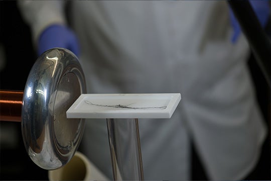
“This video is an interesting demonstration of work by Professor Hubler at University of Illinois on self-assembling wire networks. These consist of electrically polarizable particles which self assemble in response to an electric field. The optimization in self-assembling wire networks can be viewed as the network learning the nature of its environment, analogous to Hebb’s learning rule in neural networks. Learning rules are mathematical algorithms (logic) that help an evolving intelligent system, such as a biological life form, learn from the existing local conditions and improve its performance over time through iteration when exposed to new conditions. The Hebb learning rule, developed in 1949 by Donald Hebb, simply ensures “Neurons that fire together, wire together.”
Mathematically, if two neighboring neurons activate and deactivate at the same time, the weight of the connection-line between those two neurons should increase. If the neurons activate in totally opposite phases, the weight between them should decrease. If there is no signal correlation, the weight should not change. In regular Hebbian learning, the connection weights increase monotonically over time, just as the conductivity increases monotonically to infinity. In order to overcome this in modeling an adaptive self-assembling wire network, it must be able to increase the resistance of a connection naturally, or even destroy connections which are undesirable, when conditions change. In neural networks, this corresponds to having excitatory connections (which increase neuron activity) and inhibitory connections (which decrease activity). The video is a great demonstration of self-assembling wire networks.”
“Schematic illustration of hierarchical structures of carbon nanofiber bundles made of bitten warped nanographene molecules.”
https://pubs.acs.org/doi/10.1021/jacs.1c00863
https://eurekalert.org/news-releases/603291
3D design leads to first stable self-assembling nanographene wires / 3/24/21
“Nanographene is flexible, yet stronger than steel. With unique physical and electronic properties, the material consists of carbon molecules only one atom thick arranged in a honeycomb shape. Still early in technological development, current fabrication methods require the addition of substituents to obtain a uniform material. Additive-free methods result in flimsy, breakable fibers–until now. An international team of researchers has developed self-assembling, stable and strong nanographene wires. The results were published on March 24 in Journal of the American Chemical Society. The team, led by Yasutomo Segawa, associate professor at the Institute for Molecular Science, part of the National Institutes of Natural Science in Japan, set out to synthesize curved, infinitely stacking nanographenes — like potato chips in a cardboard can — that can assemble into nanowires. “Effectively stacked hydrocarbon wires have the potential to be used as a variety of nano-semiconductor materials,” Segawa said. “Previously, it has been necessary to introduce substituents that are not related to or inhibit the desired electronic function in order to control the assembly of the wires.” By removing substituents, or additives, from the fabrication process, researchers can develop molecular materials that have a specific, desired electronic function, according to Segawa. With this goal in mind, the team developed a molecule called ‘bitten’ warped nanographene (bWNG), with 68 carbon atoms and 28 hydrogen atoms forming a ‘bitten apple’ shape. Created as a solution, when left to evaporate over 24 hours in the presence of hexane — an ingredient in gasoline with six carbon atoms — bWNG becomes a gel.

“Structure of double-helix supramolecular nanofibers assembled from ‘bitten’ warped nanographenes (bWNG). (Upper left) An assembly of two bWNGs. (Lower left) Top view of a nanofiber. A double-helix with a diameter of 2.8 nm is formed with each molecule shifted by 45 degrees. (Middle) Side view of a nanofiber. (Right) Nanofiber bundles.”
The researchers attempted to recrystallize the molecules of the original solution to examine the specific structure of the bWNG gel through X-ray crystallography. This technique can reveal the atomic and molecular structure of a crystal by irradiating the structure with X-rays and observing how they diffract. “We attempted recrystallizing many times to determine the structure, but it grew to only a few hundred nanometers,” Segawa said, noting that this size is much too small for X-ray crystallography. “It was only by electron diffraction, a new method for determining the structure of organic materials, that we were able to analyze the structure.” Electron diffraction is similar to X-ray crystallography, but it uses electrons instead of X-rays, resulting in a pattern of interference with the sample material that indicates the internal structure. They found that the bWNG gel consisted of double-stranded, double-helix nanofibers that assembled themselves from curved, stackable nanographenes. “The structure of the nanofibers is a double-stranded double helix, which is very stable and, therefore, strong,” Segawa said. “Next, we would like to realize a semiconductor wire made entirely of carbon atoms.”
https://pubs.acs.org/doi/abs/10.1021/acsnano.6b02313
https://news.rice.edu/nanotubes-assemble-rice-introduces-teslaphoresis
Nanotubes assemble! Rice introduces ‘Teslaphoresis’ / 4/14/2016
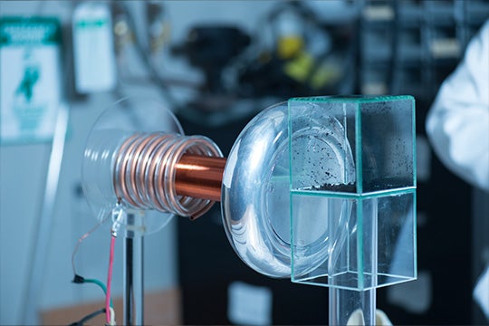
“Scientists at Rice University have discovered that the strong force field emitted by a Tesla coil causes carbon nanotubes to self-assemble into long wires, a phenomenon they call “Teslaphoresis.” The team led by Rice chemist Paul Cherukuri reported its results this week in ACS Nano. Cherukuri sees this research as setting a clear path toward scalable assembly of nanotubes from the bottom up. The system works by remotely oscillating positive and negative charges in each nanotube, causing them to chain together into long wires. Cherukuri’s specially designed Tesla coil even generates a tractor beam-like effect as nanotube wires are pulled toward the coil over long distances.

This force-field effect on matter had never been observed on such a large scale, Cherukuri said, and the phenomenon was unknown to Nikola Tesla, who invented the coil in 1891 with the intention of delivering wireless electrical energy. “Electric fields have been used to move small objects, but only over ultrashort distances,” Cherukuri said. “With Teslaphoresis, we have the ability to massively scale up force fields to move matter remotely.” The researchers discovered that the phenomenon simultaneously assembles and powers circuits that harvest energy from the field.
“wires self-assemble under the influence of a directed electric field from the Tesla coil”
In one experiment, nanotubes assembled themselves into wires, formed a circuit connecting two LEDs and then absorbed energy from the Tesla coil’s field to light them. Cherukuri realized a redesigned Tesla coil could create a powerful force field at distances far greater than anyone imagined. His team observed alignment and movement of the nanotubes several feet away from the coil. “It is such a stunning thing to watch these nanotubes come alive and stitch themselves into wires on the other side of the room,” he said. Nanotubes were a natural first test material, given their heritage at Rice, where the HiPco production process was invented. But the researchers envision many other nanomaterials can be assembled as well.
Lindsey Bornhoeft, the paper’s lead author and a biomedical engineering graduate student at Texas A&M University, said the directed force field from the bench-top coil at Rice is restricted to just a few feet. To examine the effects on matter at greater distances would require larger systems that are under development. Cherukuri suggested patterned surfaces and multiple Tesla coil systems could create more complex self-assembling circuits from nanoscale-sized particles. Cherukuri and his wife, Tonya, also a Rice alum and a co-author of the paper, noted that their son Adam made some remarkable observations while watching videos of the experiment. “I was surprised that he noticed patterns in nanotube movements that I didn’t see,” Cherukuri said. “I couldn’t make him an author on the paper, but both he and his little brother John are acknowledged for helpful discussions.” Cherukuri knows the value of youthful observation – and imagination – since he started designing Tesla coils as a teen. “I would have never thought, as a 14-year-old kid building coils, that it was going to be useful someday,” he said.
“Nanotube assemblies are drawn to the source of a Tesla field in an experiment at a Rice lab.”
Cherukuri and his team self-funded the work, which he said made it more meaningful for the group. “This was one of the most exciting projects I’ve ever done, made even more so because it was an all-volunteer group of passionate scientists and students. But because Rice has this wonderful culture of unconventional wisdom, we were able to make an amazing discovery that pushes the frontiers of nanoscience.” The teammates look forward to seeing where their research leads. “These nanotube wires grow and act like nerves, and controlled assembly of nanomaterials from the bottom up may be used as a template for applications in regenerative medicine,” Bornhoeft said. “There are so many applications where one could utilize strong force fields to control the behavior of matter in both biological and artificial systems,” Cherukuri said. “And even more exciting is how much fundamental physics and chemistry we are discovering as we move along. This really is just the first act in an amazing story.”
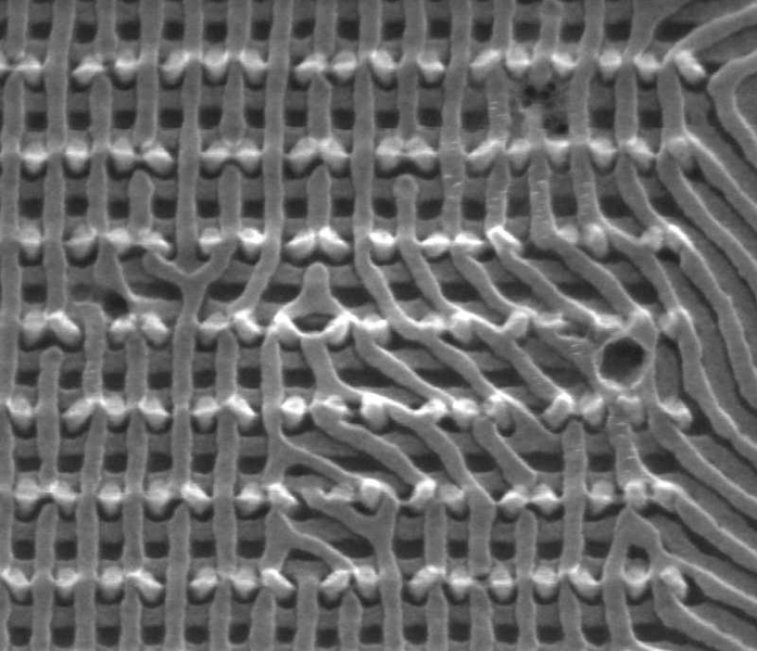
“This electron microscope image shows two layers of nanowires produced through the MIT team’s self-assembly process, showing how deviations in the pattern and connections between the layers can be included in the design.”
https://instructables.com/Self-Assembling-Wires
https://news.mit.edu/three-dimensional-self-assembling-polymers
Teaching self-assembling structures a new trick
by David L. Chandler / June 7, 2012
“Researchers at MIT have found a new way of making complex three-dimensional structures using self-assembling polymer materials that form tiny wires and junctions. The work has the potential to usher in a new generation of microchips and other devices made up of submicroscopic features.Although similar self-assembling structures with very fine wires have been produced before, this is the first time the structures have been extended into three dimensions with different, independent configurations on different layers, the researchers say. The research is published this week in the journal Science. Caroline Ross, the Toyota Professor of Materials Science and Engineering at MIT, says there has been “a lot of interest” among semiconductor researchers in finding ways to produce chip features that are much narrower than the wavelength of light — and hence narrower than what can be achieved using present light-based fabrication systems. Self-assembly based on polymers has been an active area of research, Ross says, but “what we did in this paper was push it into the third dimension.”
She and her colleagues began by creating an array of tiny posts on a substrate of silicon; they then coated the surface with materials called block copolymers, which have a natural tendency to assemble into long cylindrical structures. By carefully controlling the initial spacing of the posts, Ross explains, the researchers were able to set the spacing, angles, bends and junctions of the cylinders that form on the surface. What’s more, she says, “Each of the two layers of cylinders can be independently controlled using these posts,” making it possible to create complex 3-D configurations. Amir Tavakkoli, a visiting graduate student from the National University of Singapore and lead author of the Science paper, says many researchers have tried to produce complex arrangements of nanoscale wires through self-assembly. But earlier attempts used complex processes with many steps, and had failed to control the resulting configurations well. The new system is simpler, Tavakkoli says, and “not only controlled the alignment of the wires, but showed we can even have sharp bends and junctions” at precisely determined locations. “It wasn’t expected to be possible,” says MIT graduate student Kevin Gotrik. “It was a surprising result. We stumbled upon it, and then had to figure out how it works.”
There were a number of barriers to overcome in making the system practical, Gotrik says. For example, the posts fabricated on the surface are the key to controlling the whole self-assembly process, but they need to be quite a bit taller than they are wide, which could lead some to topple over; the MIT team ultimately found materials and shapes that would be stable. “We explored a wide range of conditions,” Gotrik says. Graduate student Adam Hannon says the team used computer simulations of the structures in order to explore the effects of different post configurations on the double-layer 3-D structure. These simulations were compared with the most promising structures observed in the laboratory to get greater insight into how to control the resulting structures that formed. So far, the MIT team has only produced two-layer configurations, but Alfredo Alexander-Katz, an assistant professor of materials science and engineering, says, “I think it would be feasible to go to three layers” while still maintaining full control over the arrangement of structures on each layer. A key enabling technology was the MIT lab’s capability, using electron-beam lithography, to make 10-nanometer-wide cylindrical posts with precisely controlled positioning. These posts, in turn, guide the positioning of the self-assembling cylinders. Karl Berggren, an associate professor of electrical engineering, says it’s as if the lithography puts down an array of pillars, and these pillars then control the complex, multilevel routing of crisscrossing highways.
In earlier work, the MIT researchers had demonstrated that this self-assembly method could be used to create wires that are much finer than those that can be made by existing photolithography techniques for producing microchips — and thus help lead the way to next-generation devices that pack even more wires and transistors into a given area of silicon chip material. “In principle, this is scalable to quite small dimensions,” Ross says, far smaller than the 15-nanometer width of the cylinders produced so far — which is already less than half the width of the finest wires in existing microchips. The basic technologies involved are compatible with existing manufacturing equipment in the semiconductor industry, the researchers say. But this is basic research that is probably still far from actual chip production, they caution. Within the next year the team hopes to use this methodology to produce a simple electronic device.
The technique is not limited to producing wires on a silicon chip, Ross and her colleagues say. The same method could be used to create 3-D arrays of other kinds of materials — such as proteins or DNA molecules, for example — in order to create biological detectors or drug-delivery systems. Craig Hawker, a professor of chemistry and biochemistry at the University of California at Santa Barbara, says this is a “far-reaching finding,” which “goes a long way to fulfilling the demands of the International Technology Roadmap for Semiconductors, which calls for a robust, commercially viable nanopatterning technique.” Hawker adds, “The robustness and power of this approach may also lead to applications outside lithography and microelectronics, with impact in water purification, membranes and organic photovoltaics.” He says this work is “a spectacular example of multidisciplinary work, with advances in chemistry, physics and nanotechnology seamlessly combined to address a critical technological and important societal problem.”
PREVIOUSLY
LIVE WIRES
https://spectrevision.net/2019/07/04/live-wires/
BACTERIAL POWER CORDS FOUND in SEABED
https://spectrevision.net/2012/10/26/bacterial-power-cords/
SWARMBOTS
https://spectrevision.net/2013/10/04/swarmbots/